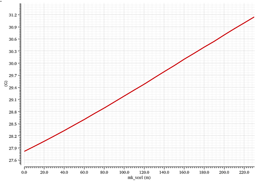
top of page

A 31GHz -99.9dBc/Hz PN, 0.4ns start-up time NMOS Cross-Coupled mm-wave LC-VCO for 5G NR applications in GF 22nm FDSOI 

VCO Schematic

VCO Hand Design

Hand Design 1.png
Hand Design 2.png

50pH Inductor Design

Screenshot from 2025-04-20 14-31-32.png
L_vs_freq__50pH_CTsymmInd.png
Q_vs_freq__50pH_CTsymmInd.png

Varactor Layout

Varactor_Layout.png

VCO Plots

VCO Tuning Range

Tuning_Range_vs_Vctrl.png

Output Power vs Oscillation Frequency

OutputPower_vs_freq_v2.png

Phase Noise vs Tuning Range

Phase_Noise_vs_Vctrl.png

Phase Noise Plots

Phase Noise Plot.png

Start-up Time

Startup_Time.png

Project Documentation (button below) includes:
1. VCO Schematics with DC Operating Points, Component Parameters
2. Main VCO Specifications (Tuning Range, Pout, PN, Start-Up time) at 65degC, 0.8V
3. Main VCO Specifications at 125degC, 0.75V
4. Main VCO Specifications for TT, FF, SS corners

bottom of page